Safeagle Industry PCB X-ray inspection System, also known as automated X-ray inspection, is a quality monitoring method for finding hidden defects in circuit boards. This technology is widely used in the medical and aerospace fields to find hidden features and identify errors such as solder bridges, solder shorts, etc.
X-ray technology stands out as the optimal method for swiftly and non-destructively examining both the internal and external structures of components with precision. Safeagle CT Solutions specializes in 3D X-ray microscope solutions, providing resolutions down to the sub-micron level for a comprehensive range of applications in both industrial and academic settings.
Our diverse portfolio of CT systems caters to a broad spectrum of analyses, offering Micro focus capabilities with a resolution of 4 µm to Nano focus precision at 0.35 µm, tailored to specific application requirements.
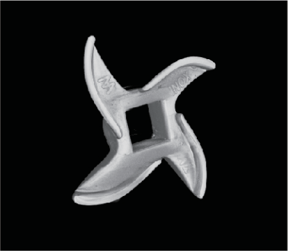
(Test examples)
Automated X-ray Inspection (AXI) is a widely used method for identifying invisible defects associated with ICs (CSP: Chip Scale Packages) and BGAs in printed circuit boards. The system uses X-rays as the scanning source. It is suitable for detecting large voids and cracks. This approach provides non-destructive access to internal geometry and structural components. AXI works in the same way as AOI by capturing images. The only difference is that AOI uses a light source, while AXI uses X-rays for scanning.
All SMDs and their solder joints can be inspected by X-ray. The machine's software creates a real-time 2D image of the component. With the help of these images, defects can be easily visualized and analyzed. The device can also find the root cause of each problem.
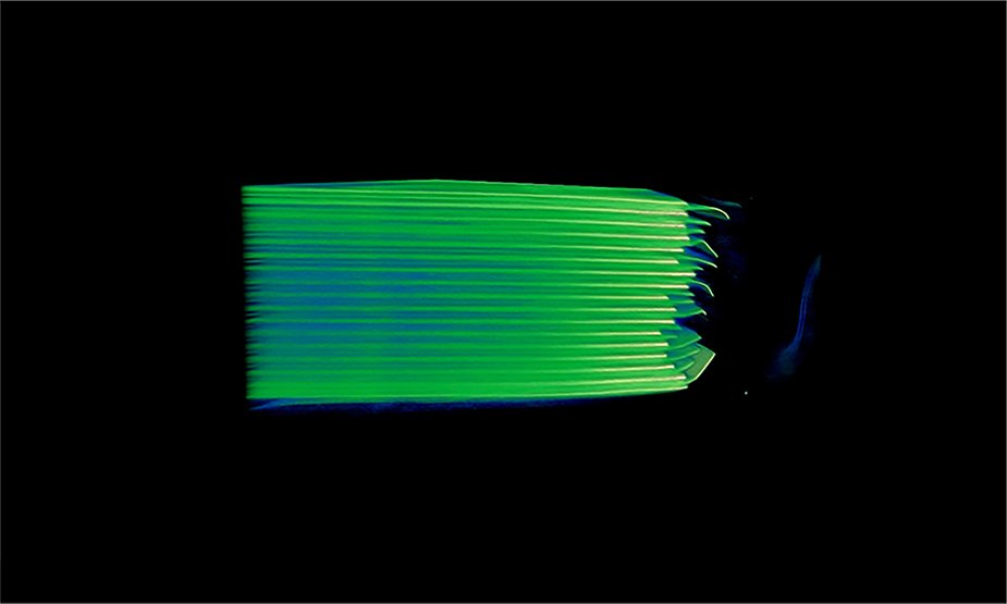
In general, the proportion of a material that absorbs X-rays is proportional to its atomic number, density, and thickness. Heavier materials absorb more X-rays than lighter materials. Such heavy materials appear darker in their images than materials that absorb very few X-rays. Lighter materials are more transparent to this radiation.
As shown in the image above, dark black areas represent materials composed of heavy elements, while transparent or relatively light areas represent materials composed of light elements. This shows that X-ray inspection is effective in identifying hidden problems such as opens, shorts, misalignments, and missing electrical components.
When it comes to PCBAs, solder joints are made of heavy materials, while other components such as packages, silicon ICs, and component leads are made of light materials. As a result, high-quality solder joints will appear darker on the image than other parts. - Safeagle Industry X-ray CT inspection System
Fill out more information, We will get back to you within 24 hours.
4F.,Bldg. B, Jin Hao Pioneer Park, No.9 Dafu Industrial Zone, Aobei Community, Guanlan St., Longhua Dist., Shenzhen, R.P.China
Sales@Safeagle.com
Telephone : 86-0755-82373580
Business Phone : 86-0755-82373580
Work Time :9:00-18:30(Beijing time)


