The infrared focal plane detector is the core component of the thermal imaging system, and it is the key to detecting, identifying and analyzing the infrared information of the object. The performance of the detector directly determines the final performance of the thermal imaging system.
Infrared focal plane detectors can be divided into two categories: refrigerated and uncooled.
The advantages of refrigerated infrared focal plane detectors are high sensitivity, ability to distinguish more subtle temperature differences, and long detection distance, but their structure is complex and costly, and they are mainly used in high-end military equipment;
The uncooled infrared focal plane detector does not require a cooling device, can work at room temperature, and has many advantages such as fast start-up, low power consumption, small size, lightweight, long life, and low cost.
Although there is a certain gap between uncooled infrared focal plane detectors and refrigerated devices in sensitivity, after more than ten years of development, it has been significantly better than refrigerated detectors in terms of cost performance, and has a broader application prospect.
Among them, the technical route of the microbolometer has defeated other types such as thermopile/thermocouple, ferroelectric, making it the mainstream technology direction of uncooled infrared focal plane detectors, and it has almost occupied the entire market share in this field.
Uncooled infrared focal plane detectors can be technically divided into three modules: microbolometer, readout circuit, and vacuum packaging. These three modules have a certain degree of independence and mutual influence, and jointly promote uncooled detectors. Technological development.
Microbolometer
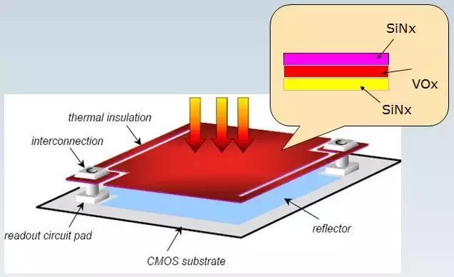
The figure above is a schematic diagram of the structure of a single microbolometer. MEMS technology is used to grow pixels very similar to the bridge deck structure on a silicon substrate, so it is also called a microbridge. The bridge deck is usually composed of multiple layers of materials, including an absorption layer for absorbing infrared radiation energy, and a heat-sensitive layer that converts temperature changes into voltage (or current) changes. The bridge arms and piers play the role of supporting the bridge deck and realizing electrical connection.
The selection of the heat-sensitive layer material has a great influence on the sensitivity of the microbolometer (NETD). The most commonly used heat-sensitive materials include vanadium oxide (VOx) and polysilicon (a-Si), and the corresponding non-refrigeration Infrared focal plane detectors are also divided into two technical camps accordingly.
In the late 1980s, Honeywell of the United States took the lead in developing an uncooled vanadium oxide microbolometer with military funding. Polysilicon technology started about ten years late. The French Atomic Energy Commission and Information Technology Laboratory/Infrared Laboratory (CEA2LETI/LIR) began to study polysilicon thin films in the early 1990s, and it took about ten years to launch polysilicon detector products.
Vanadium oxide has become the mainstream technology route of uncooled infrared focal plane detectors due to its more outstanding comprehensive performance. So far, it has occupied more than 80% of the global market, and the market share of polysilicon detectors is less than 20%.
Readout circuit
The readout circuit of the uncooled infrared focal plane detector outputs the small resistance change of each microbolometer as an electrical signal. Since the microbolometer is very sensitive to changes in the temperature of its substrate, a thermoelectric thermostat (TEC) must be used at the beginning to keep the focal plane temperature of the uncooled detector stable.
In recent years, with the improvement of readout circuit design level, some compensation circuits that suppress the temperature drift of the output signal of the pixel are gradually added to the readout circuit design, so that TEC-free applications can be realized, making the uncooled infrared focal plane detector work Consumption, volume, cost and other aspects are more advantageous.
Vacuum packaging technology
The temperature change of the microbolometer after receiving the infrared radiation of the target is very weak. In order to maintain the heat on it and avoid heat exchange with air molecules, it needs to be placed in a vacuum environment to work.
The requirements for vacuum packaging of uncooled infrared focal plane detectors are: excellent and reliable airtightness, infrared windows with high transmittance, high yield, and low cost.
The current packaging technology can be divided into metal shell, ceramic shell, wafer level, pixel level, etc. The industry often classifies detector products according to the packaging form.
Metal case package
This is the first packaging technology to be adopted, and the technology is very mature. However, due to the use of high-cost components such as metal shells, TECs, and getters, the cost has been high, which limits its application in low-cost devices.
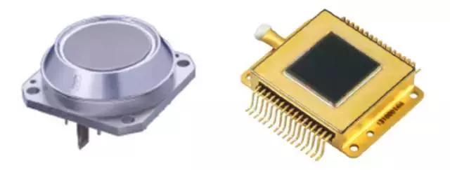
Metal shell package of the uncooled infrared focal plane
Ceramic package
This type of packaging benefits from the development of TEC-free technology, which can significantly reduce the volume and weight of the packaged detector, and the raw material cost and manufacturing cost are much lower than the traditional metal shell package, which is suitable for mass production.
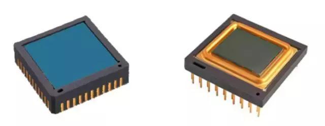
Ceramic shell package for uncooled infrared focal plane
Wafer level packaging
Wafer-level packaging is a packaging technology that has just entered the practical stage. This technology requires manufacturing another silicon window wafer corresponding to the detector wafer, accurately aligning the infrared detector chip with the silicon window, soldering the two wafers together in a vacuum chamber, and finally splitting the wafers into individual wafers. Wafer-level infrared detectors. Wafer-level packaging technology has higher integration, simpler process steps, and is more suitable for mass and low-cost production.
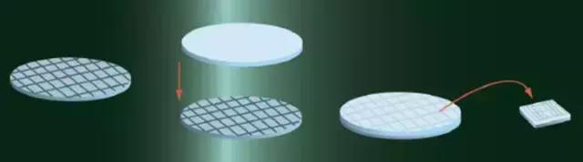
Wafer-level packaging of the uncooled infrared focal plane
Pixel-level packaging technology
It is still in the research stage, and there is still a long way to go before commercialization. This technology is equivalent to adding a packaging step in the current MEMS process, manufacturing an inverted microcap for each pixel microbridge structure in the vacuum chamber, and sealing each pixel independently. The pixel-level packaging technology integrates the packaging into the MEMS process, simplifies the manufacturing process of the uncooled infrared focal plane detector, and reduces the packaging cost to the extreme.
The core of the thermal imaging system-Uncooled infrared focal plane detector - Safeagle
Fill out more information, We will get back to you within 24 hours.
4F.,Bldg. B, Jin Hao Pioneer Park, No.9 Dafu Industrial Zone, Aobei Community, Guanlan St., Longhua Dist., Shenzhen, R.P.China
Sales@Safeagle.com
Telephone : 86-0755-82373580
Business Phone : 86-0755-82373580
Work Time :9:00-18:30(Beijing time)

